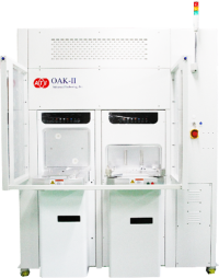
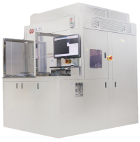
Wafer Inspection System

- High throughput with 2D and 3D optical system
- Chip inspection after sawing
- Kerf inspection
- Advanced D2D algorithm using golden die
- Verifying review module included
- Self-developed lens for wide field of view and high resolution
- Real time auto focusing module adopted
- Optional IR inspection to inspect defects, cracks and chippings inside silicon.
- Online and Offline Classification
- FAB Automation (SECS/GEM)