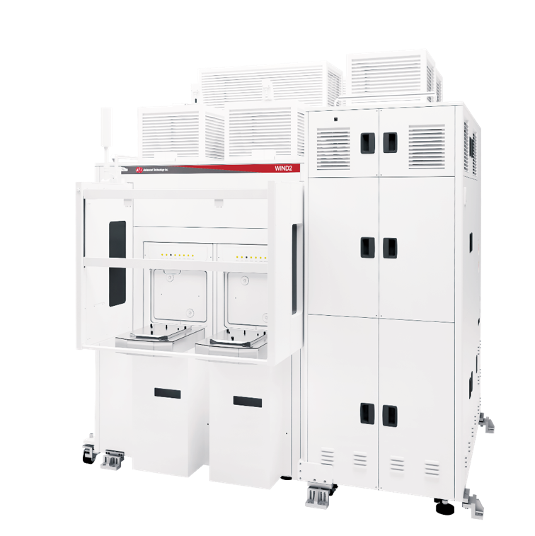
Products

You are here:-Products

Products

OAK

Auto Scope System Auto Focus 2 types of review mode(Direct, Manual) Image Saving CD Measurement Overlay KLARF / MAP file Automation Overkill Review Camera : Color Verification 1M Area Camera Scope : 5X, 10X, 20X, 50X, 100X, 150X Repeatability : 1um@3σ

By |2018-05-04T18:49:23+09:005월 4th, 2018|Categories: Semiconductor|0 Comments

Cypress

Package Inspection System 2D inspection with high resolution 3D height measurement of the attached components Multiple handling of various types of packaging JEDEC tray, SUS tray, strip, etc. IR optics for inspection through silicon

By |2018-05-04T18:41:10+09:005월 4th, 2018|Categories: Semiconductor|0 Comments

LMS-400G

Laser Marking System IC Package Substrate Reject Marking / 2D Barcode & Serial No. Marking System Reject, 2D barcode and Serial Number Marking at once on Standard Machine Available for Electrolysis / Electroless / OSP Plating Products with ATI Specialized Marking Illumination High Marking Accuracy with 10um

By |2018-05-04T18:36:11+09:005월 4th, 2018|Categories: Laser|0 Comments

AVIS-1800 Series

Automatic Final Vision Inspection for IC Package substrate. As Industry Standard AFVI, Available for Various Substrate Products Available for 2um~5.5um Resolution depends on Substrate Product Model Inspect various types of products such as BOC, CSP, UTC, SiP, PBGA, MMC, FC-CSP (Non SOP Type), BOL, FC-CSP (SOP Type,

By |2018-05-04T18:45:24+09:005월 4th, 2018|Categories: PCB|0 Comments

PINE

Automatic Final Vision Inspection for IC Package substrate. Inspect various types of products such as BOC, CSP, UTC, SiP, PBGA, MMC, FC-CSP (Non-SOP) Multiple handling of various sizes of products (W)40~120mm, (L)100~300mm, (T)0.06mm and 1.50mm High throughput with color processing

By |2018-05-04T18:29:50+09:005월 4th, 2018|Categories: PCB|0 Comments

SUN

Reticle Inspection System MASK Inspection Pellicle Top Inspection Pellicle Bottom Inspection Pellicle Frame Inspection Back Side Inspection Automated Particle Cleaning Function

By |2018-05-04T18:29:41+09:005월 4th, 2018|Categories: Semiconductor|0 Comments

WIND

Wafer Inspection System High throughput with 2D and 3D optical system Chip inspection after sawing Kerf inspection Advanced D2D algorithm using golden die Verifying review module included Self-developed lens for wide field of view and high resolution Real time auto focusing module adopted Optional IR inspection to inspect

By |2018-05-04T18:42:07+09:005월 4th, 2018|Categories: Semiconductor|0 Comments